- 您现在的位置:买卖IC网 > Sheet目录2008 > MAX1395ETB+T (Maxim Integrated Products)IC ADC 10BIT 357KSPS 10-TDFN
MAX1392/MAX1395
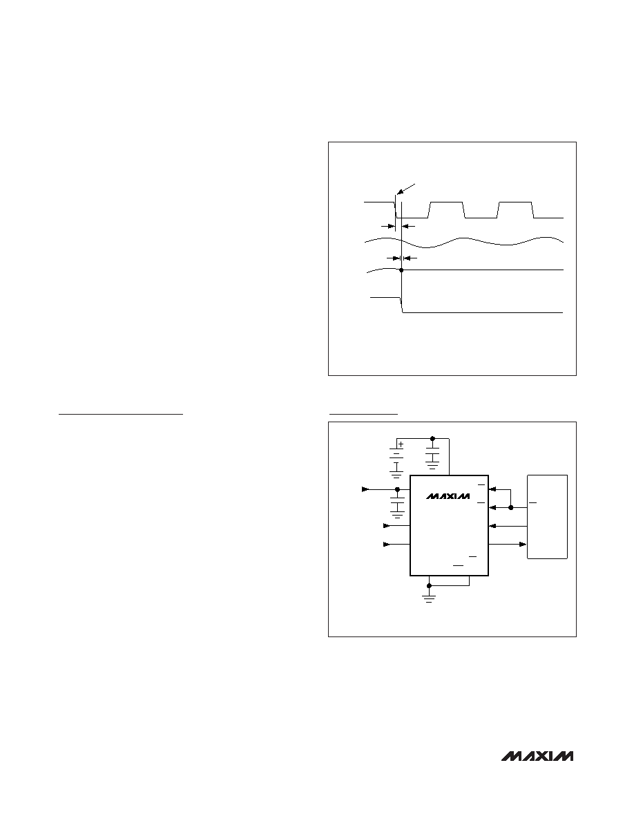
Aperture Delay
The MAX1392/MAX1395 sample data on the falling
edge of its third SCLK cycle (Figure 14). In actuality,
there is a small delay between the falling edge of the
sampling clock and the actual sampling instant.
Aperture delay (tAD) is the time defined between the
falling edge of the sampling clock and the instant when
an actual sample is taken.
Aperture Jitter
Aperture jitter (tAJ) is the sample-to-sample variation in
the aperture delay (Figure 14).
DC Power-Supply Rejection Ratio (PSRR)
DC PSRR is defined as the change in the positive full-
scale transfer function point caused by a full range vari-
ation in the analog power-supply voltage (VDD).
16
______________________________________________________________________________________
1.5V to 3.6V, 357ksps, 1-Channel True-Differential/
2-Channel Single-Ended, 10-Bit, SAR ADCs
tAD
T/H
(INTERNAL
SIGNAL)
SCLK
tAJ
TRACK
HOLD
ANALOG
INPUT
SAMPLED
DATA
THIRD FALLING EDGE
Figure 14. T/H Aperture Timing
AIN+ (AIN1)*
DOUT
SCLK
AIN- (AIN2)*
REF
INPUT
VOLTAGE
*INDICATES THE MAX1395 ONLY
2 x AA CELLS
CPU
+
-
VDD
GND
REF
INPUT
VOLTAGE
0.1
μF
0.1
μF
CS
OE
UNI/BIP
(CH1/CH2)*
MISO
SCL
SS
MAX1392
MAX1395
Typical Operating Circuit
Chip Information
TRANSISTOR COUNT: 9106
PROCESS: BiCMOS
发布紧急采购,3分钟左右您将得到回复。
相关PDF资料
MAX1400CAI+
IC ADC 18BIT LP 28-SSOP
MAX1401CAI+
IC ADC 18BIT LP 28-SSOP
MAX1415AEWE+T
IC ADC 16BIT DELTA SIGMA 16-SOIC
MAX1421CCM+D
IC ADC 12BIT 40MSPS 48LQFP
MAX1426EAI+T
IC ADC 10BITS 10MSPS 28SSOP
MAX1434ECQ+D
IC ADC 10BIT 50MSPS 100-TQFP
MAX1444EHJ+T
IC ADC 10BIT 40MSPS 32-TQFP
MAX1499ECJ+
IC ADC 3 1/2DIG W/LED DVR 32TQFP
相关代理商/技术参数
MAX1395ETB-T
功能描述:模数转换器 - ADC RoHS:否 制造商:Texas Instruments 通道数量:2 结构:Sigma-Delta 转换速率:125 SPs to 8 KSPs 分辨率:24 bit 输入类型:Differential 信噪比:107 dB 接口类型:SPI 工作电源电压:1.7 V to 3.6 V, 2.7 V to 5.25 V 最大工作温度:+ 85 C 安装风格:SMD/SMT 封装 / 箱体:VQFN-32
MAX1395MTB+T
功能描述:模数转换器 - ADC 10-Bit 2Ch 357ksps 3.6V Precision ADC RoHS:否 制造商:Texas Instruments 通道数量:2 结构:Sigma-Delta 转换速率:125 SPs to 8 KSPs 分辨率:24 bit 输入类型:Differential 信噪比:107 dB 接口类型:SPI 工作电源电压:1.7 V to 3.6 V, 2.7 V to 5.25 V 最大工作温度:+ 85 C 安装风格:SMD/SMT 封装 / 箱体:VQFN-32
MAX1395MTB-T
功能描述:模数转换器 - ADC RoHS:否 制造商:Texas Instruments 通道数量:2 结构:Sigma-Delta 转换速率:125 SPs to 8 KSPs 分辨率:24 bit 输入类型:Differential 信噪比:107 dB 接口类型:SPI 工作电源电压:1.7 V to 3.6 V, 2.7 V to 5.25 V 最大工作温度:+ 85 C 安装风格:SMD/SMT 封装 / 箱体:VQFN-32
MAX1396ETB
制造商:Maxim Integrated Products 功能描述:1.5V-3.6V312.5KSPS1-CHANNEL TRUE- - Rail/Tube
MAX1396ETB+
制造商:Maxim Integrated Products 功能描述:ADC SGL SAR 312.5KSPS 12-BIT SERL 10TDFN EP - Rail/Tube
MAX1396ETB+T
功能描述:模数转换器 - ADC 12-Bit 2Ch 312ksps 3.6V Precision ADC
RoHS:否 制造商:Texas Instruments 通道数量:2 结构:Sigma-Delta 转换速率:125 SPs to 8 KSPs 分辨率:24 bit 输入类型:Differential 信噪比:107 dB 接口类型:SPI 工作电源电压:1.7 V to 3.6 V, 2.7 V to 5.25 V 最大工作温度:+ 85 C 安装风格:SMD/SMT 封装 / 箱体:VQFN-32
MAX1396ETB-T
功能描述:模数转换器 - ADC RoHS:否 制造商:Texas Instruments 通道数量:2 结构:Sigma-Delta 转换速率:125 SPs to 8 KSPs 分辨率:24 bit 输入类型:Differential 信噪比:107 dB 接口类型:SPI 工作电源电压:1.7 V to 3.6 V, 2.7 V to 5.25 V 最大工作温度:+ 85 C 安装风格:SMD/SMT 封装 / 箱体:VQFN-32
MAX1396EUB
功能描述:模数转换器 - ADC RoHS:否 制造商:Texas Instruments 通道数量:2 结构:Sigma-Delta 转换速率:125 SPs to 8 KSPs 分辨率:24 bit 输入类型:Differential 信噪比:107 dB 接口类型:SPI 工作电源电压:1.7 V to 3.6 V, 2.7 V to 5.25 V 最大工作温度:+ 85 C 安装风格:SMD/SMT 封装 / 箱体:VQFN-32